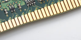
DDR4 Memory Standard

DDR4 Overview

DDR4 RAM: an Introduction to the latest DRAM Memory Technology

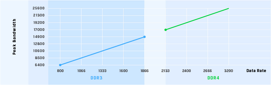
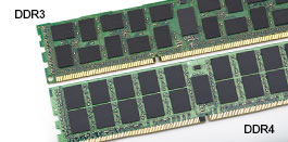
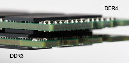
With DDR3 reaching its limits in a world that demands higher performance and increased bandwidth, a new generation of DDR SDRAM has arrived. DDR4 delivers higher performance, higher DIMM capacities, improved data integrity and lower power consumption.

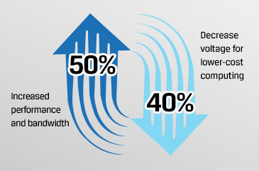
Achieving more than 2Gbps per pin and consuming less power than DDR3L (DDR3 Low Voltage), DDR4 provides up to 50 percent increased performance and bandwidth while decreasing the power consumption of your overall computing environment. This represents a significant improvement over previous memory technologies and a power savings up to 40 percent

In addition to optimized performance and greener, low-cost computing, DDR4 also provides cyclic redundancy checks (CRC) for improved data reliability, on-chip parity detection for integrity verification of ‘command and address’ transfers over a link, enhanced signal integrity and other robust RAS features.

Technology At A Glance

DDR4 Details

Please note that there are subtle differences between DDR3 and DDR4 modules.

DDR4 - Key notch difference

Key notch difference

The key notch on a DDR4 module is in a different location from the key notch on a DDR3 module. Both notches are located on the insertion edge but the notch location on the DDR4 is slightly different, to prevent it the module from being installed into an incompatible board or platform.

DDR4 - Increased thickness

Increased thickness

DDR4 modules are slightly thicker than DDR3, to accommodate more signal layers.

DDR4 - Curved edge

Curved edge

DDR4 modules feature a curved edge to help with insertion and alleviate stress on the PCB during memory installation.

Physical Features

DDR4 modules don’t look different at first glance, but there are some subtle differences. DDR4 RAM is not compatible with DDR3 motherboards and vice versa. The notch has been moved to prevent accidental insertion of the wrong type of memory. Instead of 240 pins, each module features 288 pins. To improve strength and electrical contact, there is a slight curve in the shape of the bottom of the PCB.

Faster Speeds

As for technological differences, DDR4 has faster speeds, starting at 2133MHz, which would be high-end for DDR3. Planned speed increases could take it well beyond 3200MHz.

Reduced Power Consumption

DDR4 is more efficient that DDR3, consuming up to 40% less power and requiring only 1.2V per module. This is a great benefit for notebooks, as it provides longer battery life.

Increased Capacity

DDR4 supports higher density chips and stacking technologies that may allow for single memory modules with capacities as high as 512GB.

Improved Reliability

With improved cyclic redundancy checks, on-chip parity detection of “command and address” transfers and enhanced signal integrity, DDR4 is the most reliable DDR yet.

Specifications at a Glance

DescriptionDDR3DDR4Advantage
Chip Densities 512Mb-8Gb 4Gb-16Gb Larger DIMM Capacities
Data Rates 800Mb/s – 2133Mb/s 1600Mb/s – 3200Mb/s Migration to Higher-Speed I/O
Voltage 1,5V 1,2V Reduced Memory Power Demand
Low Voltage Standard Yes (DDR3L at 1.35V) Anticipated at 1.05V Memory Power Reductions
Internal Banks 8 16 More Banks
Bank Groups (BG) 0 4 Faster Burst Accesses
VREF inputs 2 – DQs and CMD/ADDR 1 – CMD/ADDR VREFDQ Now Internal
tCK – DLL Enabled 300MHz – 800MHz 667MHz – 1,6GHz Higher Data Rates
tCK – DLL Disabled 10MHz – 125MHz (optional) Undefined to 125MHz DLL-off now fully supported
Read Latency AL + CL AL + CL Expanded Values
Write Latency AL + CWL AL + CWL Expanded Values
DQ Driver (ALT) 40 Ω 48 Ω Optimal for PtP Applications
DQ Bus SSTL15 POD12 Less I/O Noise and Power
RTT Values (in Ω) 120, 60, 40, 30, 20 240, 120, 80, 60, 48, 40, 34 Support for Higher Data Rates
RTT Not Allowed READ Bursts Disables during Read Bursts Ease-of-Use
ODT Modes Nominal, Dynamic Nominal, Dynamic, Park Add’l Control Mode; OTF Value Change
ODT Control ODT Signaling Required ODT Signaling NOT Required Ease of ODT Control; Allows Non-ODT Routing, PtP Apps
Multi-Purpose Register Four Registers – 1 Defined, 3 RFU Four Registers – 3 Defined, 1 RFU Provides Additional Specialty Readout
DIMM Types RDIMM, LRDIMM, UDIMM, SODIMM RDIMM, LRDIMM, UDIMM, SODIMM
DIMM Pins 240 (R, LR, U); 204 (SODIMM) 288 (R, LR, U); 260 (SODIMM)
RAS ECC CRC, Parity, Addressability, GDM More RAS features; improved data integrity