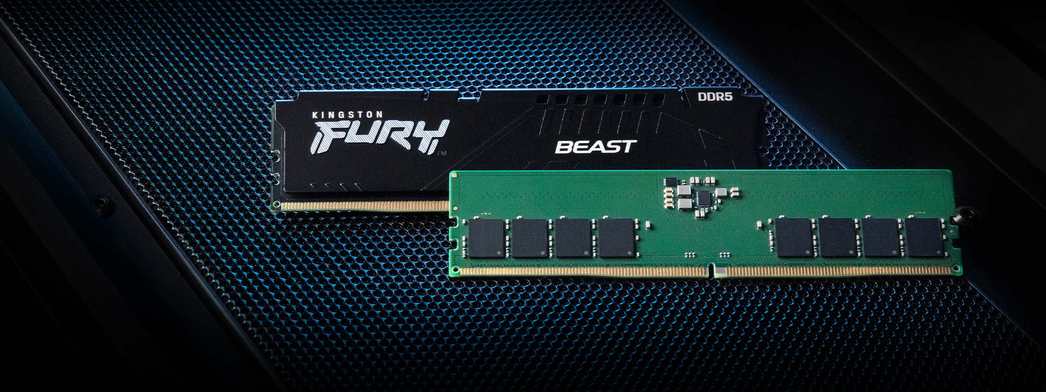
Qualified by the world's leading motherboard manufacturers{{Footnote.N64682}}
Tested and approved so you can build and upgrade with confidence on your preferred motherboard.

DDR5 is the fifth generation of Double Data Rate Synchronous Dynamic Random Access Memory, aka DDR5 SDRAM. Its development was initiated in 2017 by the industry standards body JEDEC (Joint Electron Device Engineering Council) with input from the leading global memory semiconductor and chipset architecture vendors, including Kingston. DDR5 is designed with new features for higher performance, lower power and more robust data integrity for the next decade of computing. DDR5 debuted in 2021.

DDR5 starts at 4800MT/s{{Footnote.A65242}}, while DDR4 tops out at 3200MT/s. This represents a 50% increase in bandwidth. In cadence with compute platform releases, DDR5 has planned standard speeds that will scale to 8800MT/s, possibly beyond.
At 1.1V, DDR5 consumes ~20% less power than DDR4 equivalent components at 1.2V. In addition to conserving battery life in laptops, it also has a significant advantage for enterprise servers working around the clock.
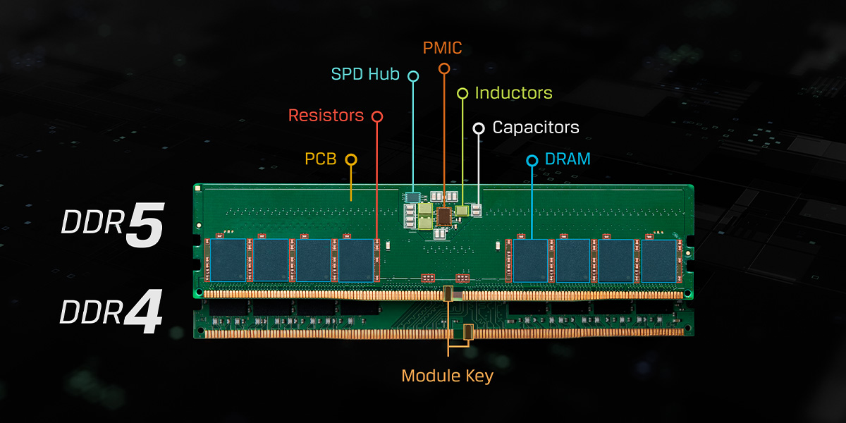
DDR5 modules feature on-board Power Management Integrate Circuits (PMIC), which help regulate the power required by the various components of the memory module (DRAM, register, SPD hub, etc). For server-class modules, the PMIC uses 12V; for PC-class modules, it uses 5V. This makes for better power distribution compared to previous generations, improves signal integrity and reduces noise.
DDR5 utilises a new device that integrates the Serial Presence Detect (SPD) EEPROM with additional hub features, manages access to the external controller and decouples the memory load on the internal bus from external.
DDR5 splits the memory module into two independent 32-bit addressable subchannels to increase efficiency and lower the latencies of data accesses for the memory controller. The data width of the DDR5 module is still 64-bit. However, breaking it down into two 32-bit addressable channels increases overall performance. For server-class memory (RDIMMs), 8-bits are added to each subchannel for ECC support for a total of 40-bits per subchannel, or 80-bits per rank. Dual rank modules feature four 32-bit subchannels.
The notch in the centre of the module acts like a key, aligning with DDR5 sockets to prevent DDR4, DDR3 or other unsupported module types from being installed. Unlike DDR4, DDR5 module keys differ between module types: UDIMM and RDIMM
On-die ECC (Error Correction Code) is a new feature designed to correct bit errors within the DRAM chip. As DRAM chips increase in density through shrinking wafer lithography, the potential for data leakage increases. On-die ECC mitigates this risk by correcting errors within the chip, increasing reliability and reducing defect rates. This technology cannot correct errors outside of the chip or those that occur on the bus between the module and memory controller housed within the CPU. ECC-enabled processors for servers and workstations feature the coding that can correct single or multi-bit errors on the fly. Extra DRAM bits must be available to allow this correction to occur, as featured on ECC-class module types such as ECC unbuffered, registered and load reduced.
Server-class DDR5 RDIMMs add temperature sensors to the ends of the modules to monitor thermal conditions across the length of the DIMM. This allows for more precise control of system cooling, as opposed to the throttling of performance seen in DDR4 for high temperatures.
DDR5 doubles the banks from 16 to 32. This allows for more pages to be open at a time, increasing efficiency. The minimum burst length is also doubled to 16, up from 8 for DDR4. This improves data bus efficiency, providing twice the data on the bus, and consequently reduces the number of reads/writes to access the same cache data line.
DDR5 adds a new command called SAME-BANK Refresh, which allows a refresh of just one bank per bank group, versus all banks. When compared to DDR4, this command allows DDR5 to further improve on performance and efficiency.
DDR5 uses Decision Feedback Equalization (DFE) to provide stable, reliable signal integrity on the module, which is required for high bandwidth.
While the memory modules themselves appear similar to DDR4, there are significant changes that make them incompatible with legacy systems. The key location (notch in the centre) moves to prevent them from being installed into incompatible sockets.

Tested and approved so you can build and upgrade with confidence on your preferred motherboard.
| Data rates (speed in MT/s){{Footnote.A65242}} | 3600, 4000, 4400, 4800, 5200, 5600, 6000, 6400, 6800, 7200, 7600, 8000, 8400, 8800 |
| Monolithic DRAM densities (Gbit) | 8Gb, 16Gb, 24Gb, 32Gb, 48Gb, 64Gb |
| Package type and ballout (x4, x8 / x16) | BGA, 3DS TSV (78, 82 / 102) |
| Interface | |
|---|---|
| Voltage (VDD / VDDQ / VPP) | 1.1 / 1.1 / 1.8 V |
| Internal VREF | VREFDQ, VREFCA, VREFCS |
| Command/Address | POD (Pseudo Open Drain) |
| Equalisation | DFE (Dynamic Feedback Equalisation) |
| Burst length | BL16 / BC8 / BL32 (optional) |
| Core architecture | |
| Number of banks | 32 banks (8 bank groups) 8 BG x 4 banks (16-64Gb x4/x8) 8 BG x 2 banks (8Gb x4/x8) 16 banks (4 bank groups) 4 BG x 4 banks (16-64Gb x16) 4 BG x 2 banks (8Gb x16) |
| Page size (x4 / x8 / x16) | 1KB / 1KB / 2KB |
| Prefetch | 16n |
| DCA (Duty Cycle Adjustment) | DQS and DQ |
| Internal DS delay monitoring | DS interval oscillator |
| ODECC (On-Die ECC) | 128b+8b SEC error check and scrub |
| CRC (Cyclic Redundancy Check) | Read/Write |
| ODT (On-Die Termination) | DS, DS, DM, CA bus |
| MIR (“Mirror” pin) | Yes |
| Bus inversion | Command/address inversion (CAI) |
| CA training, CS training | CA training, CS training |
| Write levelling training modes | Improved |
| Read training patterns | Dedicated MRs for user-defined serial, clock and LFSR-generated training patterns |
| Mode registers | Up to 256 x 8 bits |
| PRECHARGE commands | All bank, per bank and same bank |
| REFRESH commands | All bank and same bank |
| Loopback mode | Yes |
